Advancing Semiconductor Manufacturing
The University of Dayton School of Engineering is playing a role in supporting the federal government’s CHIPS and Science Act, which aims to bring semiconductor manufacturing back to the U.S., as well as create thousands of new STEM- and manufacturing-related jobs. Today, the U.S. produces about 10% of the global supply of semiconductors.

To address the need for more semiconductor manufacturing professionals, the University of Dayton School of Engineering is unveiling a new undergraduate minor in semiconductor manufacturing.
Students will collaborate with faculty experts on topics such as material and device characterization, MOSFET and CMOS design and fabrication, crystal structures, 3D transistors, EUV lithography and more.
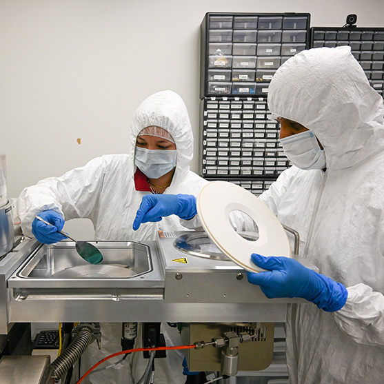
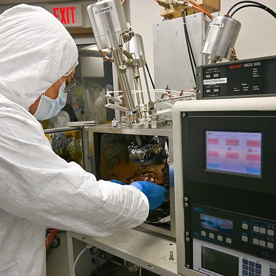
Lecture material will be complimented with hands-on lab experiences in our state-of-the-art class 100 cleanroom and the Center of Excellence for Thin-Film Research and Surface Engineering.

Through the new minor in semiconductor manufacturing, students learn from faculty experts in the field.
Dr. Andrew Sarangan: Dr. Sarangan’s work includes novel concepts in optical thin films, phase change materials and nanofabrication. His prior work includes development of a large-area nanoscale lithography using laser interference, glancing angle deposition of nanostructured thin films and vanadium dioxide and GST phase change materials.
Dr. Swapnajit Chakravarty: Dr. Chakravarty’s research focuses on semiconductor photonic integrated circuits and nanophotonic devices for applications in chemical and biological sensing, and high speed data communications in the near-infrared and mid-infrared wavelengths of the electromagnetic spectrum.
Dr. Guru Subramanyam: Dr. Guru Subramanyam's research is in the areas of thin films for electronics, photonics, energy and sensors. He is providing the leadership for UD's Center of Excellence for Thin film Research and Surface Engineering (CETRASE).
Dr. Alex Watson: Dr. Watson's research focuses on microfabrication of reconfigurable devices that integrate liquids and electronics. His prior work involved electrowetting tunable liquid optics and liquid-metal microfluidics for reconfigurable RF systems. He currently studies flexible, stretchable and wearable electronics.
Nine undergraduate students from universities across the U.S. spent their summer at UD through the National Science Foundation’s Research Experiences for Undergraduate Students (REU) program.
REU students spent 10 weeks performing research and receiving training in semiconductor materials, electronic and photonic devices and manufacturing in faculty-led labs.
They also completed Intel’s OASiS certification and sat in on luncheons to learn about semiconductors, graduate school and a future career in research. In addition, students met with the University Program Director at Intel who advised students on numerous potential career avenues both in academia and industry.
A team of faculty have recently been awarded a Major Research Instrumentation (MRI) grant from the National Science Foundation (NSF), for $390k, to purchase new equipment that will drastically reduce the time it takes UD researchers, faculty and students to create a semiconductor chip.
A direct-write laser beam lithography (LBL) system will enable researchers to move from conceptual design to a physical pattern on silicon in hours instead of weeks with significantly lower cost. It will also enable fast turnaround of semiconductor designs made by students for immediate fabrication in UD's nanofabrication cleanroom.

Dr. Guru Subramanyam, professor of electrical and computer engineering, is working on two research projects in semiconductors with the Air Force Research Laboratory.
Memristor Devices for Neuromorphic Computing:
The group has been researching memristor devices based on various oxides, and chalcogenides. Their current research focus is on developing scalable memristor devices on silicon substrates for long-term stability and reliability with potential for tens of thousands of read and write cycles and suitable for low-power neuromorphic computing.
Thin film Varactor Devices:
The group developed a patented variable-capacitor (varactor) technology using Barium Strontium Titanate (BST) thin film. These varactor devices are key components in improving broadband communication systems’ performance. The group is currently part of a team performing phase 2 demonstration of a DARPA Wide-band Adaptive RF Protection (WARP) program led by Indiana Microelectronics. Lockheed Martin Corporation, and 3D Glass Solutions Inc are the other industry partners in this project. The group is responsible for fabricating and delivering BST varactors for the chip-scale tunable filters in this project.

Dr. Swapnajit Chakravarty, associate professor of electro-optics and photonics, is leading a National Science Foundation project with the goal of developing a low-cost, hand-held device to test for and identify diseases and biohazards.
The key to reducing cost is enabling the sensor to work using a single-wavelength laser rather than more expensive wavelength-tunable lasers.
While the COVID-19 pandemic demonstrated the need for this type of testing, a device like this also could be used to identify pollutants in water, or cancers or illegal drugs by the laser “seeing” what is in a drop of blood or saliva, or someone’s breath. The sample would be placed on something that looks like a USB drive and then plugged into the portable device, he added. Results would be displayed in a few minutes.

